Description
⚙️ Product Overview
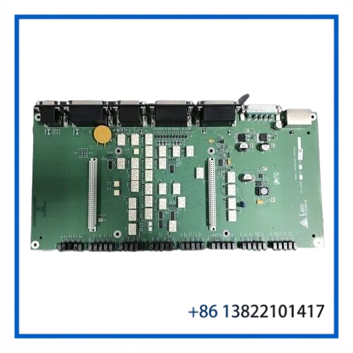
The LAM Research 810-072687-410 is a Node 1 Interlock Control PCB designed for integration into Lam Research semiconductor processing equipment. Industry spare-parts references identify the part specifically as a PCB assembly for Node 1 interlock control, while the broader 810-072687 family is listed as an interlock control board associated with Node Board Type 3 systems.
The board belongs to the equipment-level control and safety-interlock architecture rather than being a general-purpose PLC I/O card. Its role is to participate in the machine’s interlock logic, helping the equipment controller determine whether defined operating conditions are satisfied before selected machine functions are permitted.
The exact connector pinout, voltage levels, processor or logic devices, and supported equipment models are not reliably documented in public technical sources. For replacement work, the complete part number and board revision should therefore be matched against the original unit.
🔧 Key Features
- Lam Research equipment-specific control PCB
- Node 1 interlock control function
- Part Number: 810-072687-410
- Associated with the 810-072687 interlock-control family
- Used in semiconductor manufacturing equipment
- Designed for machine interlock and equipment-status control
- Suitable for legacy Lam Research equipment maintenance
- Board-level replacement for equipment service applications
- Related references include Node Board Type 3 configurations
A related equipment reference also associates a Node 1 Interlock Control Unit with 810-072687-410 and 810-800256-107, which is useful when checking a complete assembly against individual PCB markings.
📋 Product Datasheet
| Parameter | Specification |
|---|---|
| Brand | LAM Research |
| Part Number | 810-072687-410 |
| Product Type | Node 1 Interlock Control PCB |
| Board Function | Interlock / equipment control |
| System | Lam Research semiconductor equipment |
| Node | Node 1 |
| Related Family | 810-072687 Interlock Control |
| Related Architecture | Node Board Type 3 |
| Processor / Logic | Configuration-dependent; verify actual board |
| I/O Channels | Not publicly confirmed |
| Communication Interface | Verify actual board and equipment |
| Input Voltage | Verify equipment documentation |
| Output Ratings | Verify actual board |
| Firmware | Equipment/revision dependent |
| Dimensions | Verify actual unit |
| Weight | Approx. 0.85 kg reported for the PCB listing |
| Condition | Verify specific unit/listing |
The approximately 0.85 kg figure is reported by an industrial spare-parts listing for this exact part number. Electrical specifications should not be inferred from that listing.
⚡ Operating Function
An interlock PCB is normally positioned between equipment sensors, control circuits, and the main machine-control architecture.
A simplified signal path is:
Equipment Sensors / Status Signals → Interlock Control PCB → Node Control Logic → Equipment Controller
The board processes or distributes interlock-related signals so the host system can determine whether an operating condition is acceptable.
Typical interlock logic in semiconductor equipment may involve conditions such as access status, subsystem readiness, equipment faults, or other machine-permission signals. However, the exact interlock logic implemented by 810-072687-410 depends on the Lam Research tool configuration, so individual safety functions should not be assigned without the applicable equipment documentation.
This distinction matters during troubleshooting. An interlock alarm does not necessarily mean the PCB itself has failed. A sensor, cable, connector, downstream device, or machine condition can also prevent the interlock chain from reaching the required state.
🔩 Installation & Configuration
Replacement should be performed by personnel familiar with the specific Lam Research platform.
Recommended procedure:
- Shut down the equipment according to the applicable service procedure.
- Isolate electrical power before removing the PCB.
- Record the original board position and connector arrangement.
- Photograph cable routing and connector locations.
- Confirm the complete part number: 810-072687-410.
- Compare revision markings with the existing board.
- Inspect connectors for contamination, bent pins, oxidation, or mechanical damage.
- Use appropriate ESD protection when handling the PCB.
- Install the replacement in the original Node 1 position.
- Reconnect cables exactly according to the equipment documentation.
- Restore power and check controller diagnostics.
- Verify interlock status before starting normal process operation.
- Test the affected equipment sequence under controlled conditions.
Do not bypass or defeat an equipment interlock simply to determine whether the replacement board is operating. Interlock circuits are part of the machine’s protective control architecture.
🧰 Maintenance Recommendations
For an older semiconductor-tool PCB, connector condition is worth checking before replacing electronic components. Oxidation, contamination, loose contacts, and damaged cable assemblies can produce symptoms that look like a board failure.
Visual inspection: Check for burned components, cracked solder joints, damaged connectors, corrosion, and contamination.
ESD handling: Store spare boards in ESD-safe packaging and avoid touching exposed contacts.
Connector checks: Inspect mating connectors and cable assemblies before installing a replacement PCB.
Interlock diagnostics: Record the actual interlock state and alarm information. A persistent interlock fault should be traced through the complete signal chain.
Revision control: Keep the exact part number and revision in the spare-parts database. Similar-looking Lam boards can perform completely different functions.
Spare storage: Store the PCB in a dry, controlled environment and protect it from mechanical shock and static discharge.
For a used replacement board, functional verification of the relevant interlock circuits is preferable to a simple power-on check.
❓ FAQ
Q: What is LAM 810-072687-410?
It is a Lam Research Node 1 Interlock Control PCB used in semiconductor equipment. Multiple industrial references identify the exact part number with this description.
Q: Is it a general PLC I/O module?
No. It is an equipment-specific interlock/control PCB designed for Lam Research equipment.
Q: What is the 810-072687 family?
The 810-072687 family is associated with Lam Research interlock control boards. Spare-parts references also identify versions used with Node Board Type 3 configurations.
Q: Is 810-072687-410 interchangeable with 810-072687-003?
Not automatically. Both belong to the same broader interlock-control family, but the complete part number, revision, node configuration, connectors, and host equipment must be checked before substitution.
Q: What should I verify before purchasing a replacement?
Check the complete 810-072687-410 marking, PCB revision, connector arrangement, physical condition, and the exact Lam Research equipment model.
Q: Can an interlock PCB be tested outside the machine?
Basic electrical inspection may be possible, but meaningful functional testing normally requires the appropriate test setup or host equipment. The complete interlock chain should be verified rather than testing the PCB in isolation.
🔄 Related LAM Research Models & Components
- LAM Research 810-072687-410 — Node 1 Interlock Control PCB
- LAM Research 810-072687 — Interlock Control Board
- LAM Research 810-072687-003 Rev. B — Interlock Control Board
- LAM Research 810-800256-107 — related Node 1 assembly reference
- LAM Research 810-800256-207 — Node Board Type 3
- LAM Research 810-800256-015 — Node Type 3 PCB Assembly
- LAM Research 810-802901-300 — Node 1 Common Control Board
- LAM Research 810-802902-036 — Node 2 PM/HE Motherboard
- LAM Research 810-370066 — Interlock 8-Sided PM Board
- LAM Research 810-800031-345 — System Interlock VIOP PCB
These parts are related to Lam Research control, node, or interlock architectures, but they should not be considered direct replacements for 810-072687-410 without equipment-level compatibility verification.
🏭 Application Summary
The LAM 810-072687-410 is a specialized Node 1 Interlock Control PCB for Lam Research semiconductor equipment. Its importance is less about standalone computing capability and more about reliable communication of equipment interlock and permission states within the machine control architecture.
For replacement inventory, the safest identification sequence is:
LAM Research → 810-072687-410 → Node 1 Interlock Control → Board Revision → Host Equipment Model
Public listings show both pre-owned and parts-condition examples of this part, so the actual board condition should always be verified separately from the part-number identification.